Students can Download Physics Chapter 9 Semiconductor Electronics Questions and Answers, Notes Pdf, Samacheer Kalvi 12th Physics Solutions Guide Pdf helps you to revise the complete Tamilnadu State Board New Syllabus and score more marks in your examinations.
Tamilnadu Samacheer Kalvi 12th Physics Solutions Chapter 9 Semiconductor Electronics
Samacheer Kalvi 12th Physics Semiconductor Electronics Textual Evaluation Solved
Samacheer Kalvi 12th Physics Semiconductor Electronics Multiple Choice Questions
Question 1.
The barrier potential of a silicon diode is approximately,
(a) 0.7 V
(b) 0.3 V
(c) 2.0 V
(d) 2.2 V.
Answer:
(a) 0.7 V
Question 2.
Doping a semiconductor results in
(a) The decrease in mobile charge carriers
(b) The change in chemical properties
(c) The change in the crystal structure
(d) The breaking of the covalent bond.
Answer:
(c) The change in the crystal structure
![]()
Question 3.
A forward biased diode is treated as-
(a) An open switch with infinite resistance
(b) A closed switch with a voltage drop of 0V
(c) A closed switch in series with a battery voltage of 0.7V
(d) A closed switch in series with a small resistance and a battery.
Answer:
(d) A closed switch in series with a small resistance and a battery.
Question 4.
If a half – wave rectified voltage is fed to a load resistor, which part of a cycle the load current will flow?
(a) 0° – 90°
(b) 90° – 180°
(c) 0° – 180°
(d) 0° – 360°
Answer:
(c) 0° – 180°
Question 5.
The primary use of a zener diode is-
(a) Rectifier
(b) Amplifier
(c) Oscillator
(d) Voltage regulator.
Answer:
(d) Voltage regulator.
Question 6.
The principle in which a solar cell operates-
(a) Diffusion
(b) Recombination
(c) Photovoltaic action
(d) Carrier flow.
Answer:
(c) Photovoltaic action
Question 7.
The light emitted in an LED is due to-
(a) Recombination of charge carriers
(b) Reflection of light due to lens action
(c) Amplification of light falling at the junction.
Answer:
(a) Recombination of charge carriers
![]()
Question 8.
When a transistor is fully switched on, it is said to be-
(a) Shorted
(b) Saturated
(c) Cut – off
(d) Open.
Answer:
(b) Saturated
Question 9.
The specific characteristic of a common emitter amplifier is-
(a) High input resistance
(b) Low power gain
(c) Signal phase reversal
(d) Low current gain.
Answer:
(c) Signal phase reversal
Question 10.
To obtain sustained oscillation in an oscillator,
(a) Feedback should be positive
(b) Feedback factor must be unity
(c) Phase shift must be 0 or 2π
(d) All the above.
Answer:
(d) All the above.
Question 11.
If the input to the NOT gate is A = 1011, its output is?
(a) 0100
(b) 1000
(c) 1100
(d) 0011.
Answer:
(a) 0100
Question 12.
The electrical series circuit in digital form is-
(a) AND
(b) OR
(c) NOR
(d) NAND.
Answer:
(a) AND
![]()
Question 13.
Which one of the following represents forward bias diode? (NEET)
Answer:
Question 14.
The given electrical network is equivalent to (NEET)
(a) AND gate
(b) OR gate
(c) NOR gate 1
(d) NOT gate.
Answer:
(c) NOR gate
Question 15.
The output of the following circuit is 1 when the input ABC is (NEET 2016)
(a) 101
(b) 100
(c) 110
(d) 010.
Answer:
(a) 101
Samacheer Kalvi 12th Physics Semiconductor Electronics Short Answer Questions
Question 1.
Define electron motion in a semiconductor?
Answer:
To move the hole in a given direction, the valence electrons move in the opposite direction. Electron flow in an N – type semiconductor is similar to electrons moving in a metallic wire. The N – type dopant atoms will yield electron available for conduction.
Question 2.
Distinguish between intrinsic and extrinsic semiconductors.
Answer:
1. Intrinsic:
- These are pure semiconducting tetravalent crystals.
- Their electrical conductivity is low.
- There is no permitted energy state between valence and conduction band.
- Their electrical conductivity depends on temperature.
2. Extrinsic:
- These are semiconducting tetravalent crystals doped with impurity atoms group III (or) V.
- Their electrical conductivity is high.
- There is no permitted energy state of the impurity atom between valence and conduction band.
- Their electrical conductivity depends on temperature as well as dopant concentration.
Question 3.
What do you mean by doping?
Answer:
The process of adding impurities to the intrinsic semiconductor is called doping.
![]()
Question 4.
How electron-hole pairs are created in a semiconductor material?
Answer:
The free electrons from electron hole pairs, enable current to flow in the semiconductor when an external voltage is applied. The holes in the valence band also allow electron movement within the valence band itself and this also contributes to current flow. This process is called electron – hole pair generation.
Question 5.
A diode is called as a unidirectional device. Explain?
Answer:
Diode is called as a unidirectional device, i.e., current flows in only one direction (anode to cathode internally) when a forward voltage is applied, the diode conducts and when reverse voltage is applied, there is no conduction. A mechanical analogy is a rat chat, which allows motion in one direction only.
Question 6.
What do you mean by leakage current in a diode?
Answer:
The leakage current in a diode is the current that the diode will leak when a reverse voltage is applied to it. Under the reverse bias, a very small current in μA, flows across the junction. This is due to the flow of the minority charge carriers called the leakage current or reverse saturation current.
![]()
Question 7.
Draw the output waveform of a full wave rectifier.
Answer :
Question 8.
Distinguish between avalanche and zener breakdown.
Answer:
1. Avalanche Breakdown:
- It occurs in junctions which are lightly and have wide depletion widths.
- It occurs at higher reverse voltages when thermally generated electrons get enough kinetic energy to produce more electrons by collision.
- At reverse voltage above 6 V breakdown is due to avalanche effect.
- Electric field produced is weak in nature.
- Charge carriers obtain energy from the applied potential.
2. Zener Breakdown:
- It occurs in junctions which are heavily doped and have narrow depletion widths.
- It occurs due to rupture of covalent bonds by strong electric fields set up in depletion region by the reverse voltage.
- At reverse voltage below 6V breakdown is due to zener effect.
- A strong electric field is produced
- Zener current is independent of applied voltage.
Question 9.
Discuss the biasing polarities in an NPN and PNP transistors.
Answer:
In a PNP transistor, base and collector will be negative with respect to emitter indicated by the middle letter N whereas base and collector will be positive in an NPN transistor [indicated by the middle letter P]
Question 10.
Explain the current flow in a NPN transistor?
Answer:
- The conventional flow of current is based on the direction of the motion of holes
- In NPN transistor, current enters from the base into the emitter.
Question 11.
What is the phase relationship between the AC input and output voltages in a common emitter amplifier? What is the reason for the phase reversal?
Answer:
In a common emitter amplifier, the input and output voltages are 180° out of phase or in, opposite phases. The reason for this can be seen from the fact that as the input voltage rises, so the current increases through the base circuit.
![]()
Question 12.
Explain the need for a feedback circuit in a transistor oscillator.
Answer:
The circuit used to feedback a portion of the output to the input is called the feedback network. If the portion of the output fed to the input is in phase with the input, then the magnitude of the input signal increases. It is necessary for sustained oscillations.
Question 13.
Give circuit symbol, logical operation, truth table, and Boolean expression of-
- AND
- OR
- NOT
- NAND
- NOR
- EX – OR gates.
Answer:
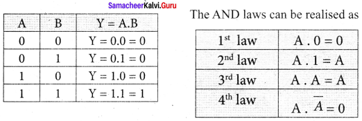
1. AND gate Circuit symbol:
A and B are inputs and Y is the output.
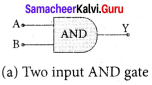
It is a logic gate and hence A, B, and Y can have the (a) Two input AND gate value of either 1 or 0.
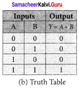
Boolean equation:
Y = A.B
It performs logical multiplication and is
different from arithmetic multiplication.
Logic operation:
The output of AND gate is high (1) only when all the inputs are high (1). The rest of the cases the output is low. Hence the output of AND gate is high (1) only when all the inputs are high.
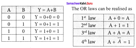
2. OR gate:
Circuit Symbol
A and B are inputs and Y is the output.
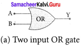
Boolean equation:
A + B = Y
It performs logical addition and is different from arithmetic addition.
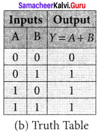
Logic operation:
The output of OR gate is high (logic 1 state) when either of the inputs or both are high.
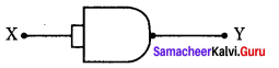
3. NOT gate:
Circuit symbol
A is the input and Y is the output.
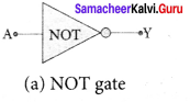
Boolean equation:
Y = \(\overline { A } \)
Logic operation:
The output is the complement of the input.
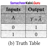
It is represented with an overbar. It is also called as inverter. The truth table infers that the output Y is 1 when input A is 0 and vice versa. The truth table of NOT.
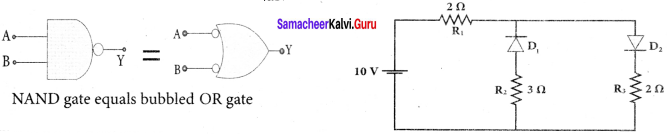
4. NAND gate:
A and B are inputs and Y is the output.
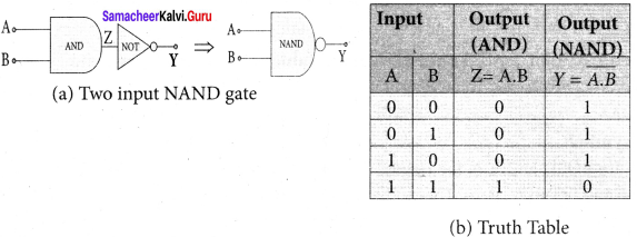
Boolean equation:
Y = Y= \(\overline { AB } \)
Logic operation:
The output Y equals the complement of AND operation. The circuit is an AND gate followed by a NOT gate. Therefore, it is summarized as NAND. The output is at logic zero only when all the inputs are high. The rest of the cases, the output is high (Logic 1 state).
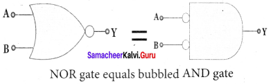
5. NOR gate:
Circuit symbol: A and B are inputs and Y is the output.
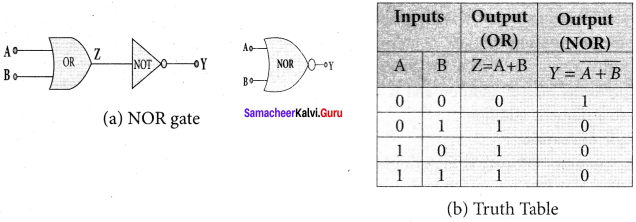
Boolean equation:
Y= A + B
Logic operation:
Y equals the complement of OR operation (A OR B). The circuit is an OR gate followed by a NOT gate and is summarized as NOR. The output is high when all the inputs are low. The output is low for all other combinations of inputs.
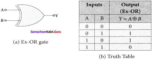
6. Ex – OR gate:
Circuit symbol
A and B are inputs and Y is the output. The Ex-OR operation is denoted as ⊕.
Boolean equation:
Y = A. \(\overline { B } \) + \(\overline { A } \) .B
Y = A ⊕ B
Logic operation:
The output is high only when either of the two inputs is high. In the case of an Ex-OR gate with more than two inputs, the output will be high when odd number of inputs are high.
Question 14.
State De Morgan’s first and second theorems De Morgan’s First Theorem?
Answer:
The first theorem states that the complement of the sum of two logical inputs is equal to the product of its complements.
\(\overline { A+B } \) = \(\overline { A } \).\(\overline { B } \)
De Morgan’s Second Theorem:
The second theorem states that the complement of the product of two inputs is equal to the sum of its complements.
\(\overline { A.B } \) = \(\overline { A+B } \)
Samacheer Kalvi 12th Physics Semiconductor Electronics Long Answer Questions
Question 1.
Elucidate the formation of a N – type and P – type semiconductors.
Answer:
1. N – type semiconductor:
A n-type semiconductor is obtained by doping a pure Germanium (or Silicon) crystal with a dopant from group V pentavalent elements like Phosphorus, Arsenic, and Antimony. The dopant has five valence electrons while the Germanium atom has four valence electrons.
During the process of doping, a few of the Germanium atoms are replaced by the group V dopants. Four of the five valence electrons of the impurity atom are bound with the 4 valence electrons of the neighbouring replaced Germanium atom. The fifth valence electron of the impurity atom will be loosely attached with the nucleus as it has not formed the covalent bond.
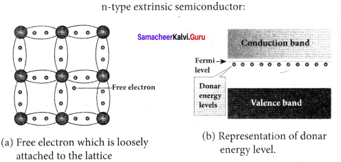
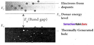
The energy level of the loosely attached fifth electron from the dopant is found just below the conduction band edge and is called the donor energy level. At room temperature, these electrons can easily move to the conduction band with the absorption of thermal energy. It is shown in the figure (c). Besides, an external electric field also can set free the loosely bound electrons and lead to conduction.
It is important to note that the energy required for an electron to jump from the valence band to the conduction band (Eg) in an intrinsic semiconductor is 0.7 eV for Ge and 1.1 eV for Si, while the energy required to set free a donor electron is only 0.01 eV for Ge and 0.05 eV for Si.
The group V pentavalent impurity atoms donate electrons to the conduction band and are called donor impurities. Therefore, each impurity atom provides one extra electron to the conduction band in addition to the thermally generated electrons. These thermally generated electrons leave holes in valence band. Hence, the majority carriers of current in an n-type Semiconductor are electrons and the minority carriers are holes. Such a semiconductor doped with a pentavalent impurity is called an n-type semiconductor.
2. P – type semiconductor:
Here, a trivalent atom from group III elements such as Boron, Aluminium, Gallium and Indium is added to the Germanium or Silicon substrate. The dopant with three valence electrons are bound with the neighbouring Germanium atom as shown in Figure (a). As Germanium atom has four valence electrons, one electron position of the dopant in the Germanium crystal lattice will remain vacant. The missing electron position in the covalent bond is denoted as a hole.
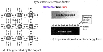
To make complete covalent bonding with all four neighbouring atoms, the dopant is in need of one more electron. These dopants can accept electrons from the neighbouring atoms. Therefore, this impurity is called an acceptor impurity. The energy level of the hole created by each impurity atom is just above the valence band and is called the acceptor-energy level, as shown in Figure (b).
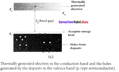
For each acceptor atom, there will be a hole in the valence band in addition to the thermally generated holes. In such an extrinsic semiconductor, holes are the majority carriers and thermally generated electrons are minority carriers. The semiconductor thus formed is called a p – type semiconductor.
![]()
Question 2.
Explain the formation of PN junction diode. Discuss its V-I characteristics.
Answer:
Formation of depletion layer:
A p – n junction is formed by joining n-type and p-type semiconductor materials as shown in figure.
(a) Since the n-region has a high electron concentration and the p-region a high hole concentration, electrons diffuse from the n-side to the p-side. This causes diffusion current which exists due to the concentration difference of electrons. The electrons diffusing into the p-region may occupy holes in that region and make it negative.
The holes left behind by these electrons in the n-side are equivalent to the diffusion of holes from the p-side to the n-side. If the electrons and holes were not charged, this diffusion process would continue until the concentration of electrons and holes on the two sides were the same, as happens if two gasses come into contact with each other.
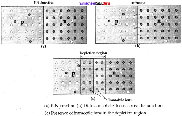
But, in a p – n junction, when the electrons and holes move to the other side of the junction, they leave behind exposed charges on dopant atom sites, which are fixed in the crystal lattice and are unable to move. On the n-side, positive ion cores are exposed and on the p-side, negative ion cores are exposed as shown in Figure
(b) An electric field E forms between the positive ion cores in the n – type material and negative ion cores in the p-type material. The electric field sweeps free carriers out of this region and hence it is called depletion region as it is depleted of free carriers. A barrier potential Vb due to the electric field E is formed at the junction as shown in Figure.
(c) As this diffusion of charge carriers from both sides continues, the negative ions form a layer of negative space charge region along the p-side. Similarly, a positive space charge region is formed by positive ions on the n-side. The positive space charge region attracts electrons from p-side to n-side and the negative space charge region attracts holes from n-side to p-side.
This moment of earners happen in this region due to the formed electric field and it constitutes a current called drift current. The diffusion current and drift current flow in the opposite direction and at one instant they both become equal. Thus, a p – n junction is formed.
V-I characteristics of a junction diode:
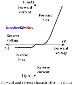
Forward characteristics:
It is the study of the variation in current through the diode with respect to the applied voltage across the diode when it is forward biased. An external resistance (R) is used to limit the flow of current through the diode. The voltage across the diode is varied by varying the biasing voltage across the dc power supply.
The forward bias voltage and the corresponding forward bias current are noted. A graph is plotted by taking the forward bias voltage (V) along the X – axis and the current (I) through the diode along the Y – axis. This graph is called the forward V-I characteristics of the p – n junction diode. Three inferences can be brought out from the graph:
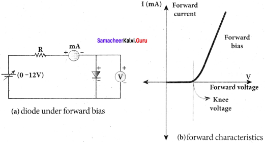
(i) At room temperature, a potential difference equal to the barrier potential is required before a reasonable forward current starts flowing across the diode. This voltage is known as threshold voltage or cut-in voltage or knee voltage (Vth). It is approximately 0.3 V for Germanium and 0.7 V for Silicon. The current flow is negligible when the applied voltage is less than the threshold voltage. Beyond the threshold voltage, increase in current is significant even for a small increase in voltage.
(ii) The graph clearly infers that the current flow is not linear and is exponential. Hence it does not obey Ohm’s law.
(iii) The forward resistance (rf) of the diode is the ratio of the small change in voltage (∆V)to the small change in current(∆I), rf = \(\frac { ∆V }{ ∆I }\)
However, if the applied voltage is increased beyond a rated value, it will produce an extremely large current which may destroy the junction due to overheating. This is called as the breakdown of the diode and the voltage at which the diode breaks down is called the breakdown voltage. Thus, it is safe to operate a diode well within the threshold voltage and the breakdown voltage.
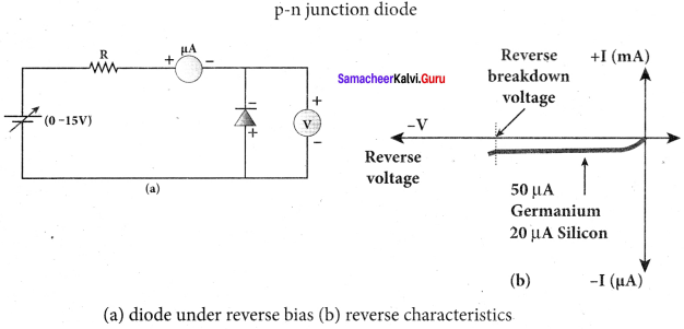
Reverse characteristics:
In the reverse bias, the p-region of the diode is connected to the negative terminal and n-region to the positive terminal of the dc power supply. A graph is drawn between the reverse bias voltage and the current across the junction, which is called the reverse characteristics of a p-n junction diode.
Under this bias, a very small current in μA, flows across the junction. This is due to the flow of the minority charge carriers called the leakage current or reverse saturation current. Besides, the current is almost independent of the voltage. The reverse bias voltage can be increased only up to the rated value otherwise the diode will enter into the breakdown region.
Question 3.
Draw the circuit diagram of a half wave rectifier and explain its working Half wave rectifier circuit:
Answer:
The half wave rectifier circuit. The circuit consists of a transformer, a p-n junction diode and a resistor. In a half wave rectifier circuit, either a positive half or the negative half of the AC input is passed through while the other half is blocked. Only one half of the input wave reaches the output. Therefore, it is called half wave rectifier. Here, a p-n junction diode acts as a rectifying diode.
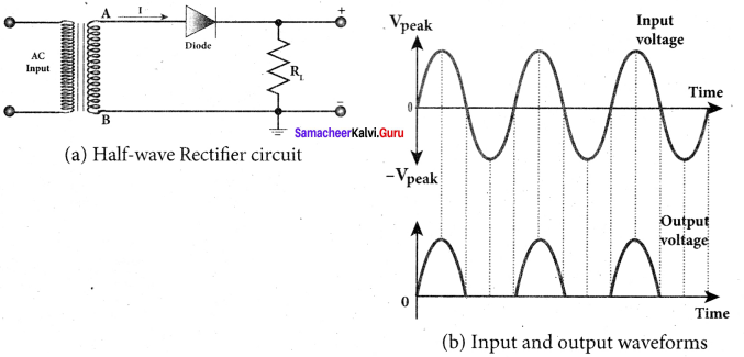
During the positive half cycle:
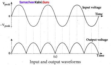
When the positive half cycle of the ac input signal passes through the circuit, terminal A becomes positive with respect to terminal B. The diode is forward biased and hence it conducts. The current flows through the load resistor RL and the AC voltage developed across RL constitutes the output voltage V0 and the waveform of the diode current.
During the negative half cycle:
When the negative half cycle of the ac input signal passes through the circuit, terminal A is negative with respect to terminal B. Now the diode is reverse biased and does not conduct and hence no current passes through RL. The reverse saturation current in a diode is negligible. Since there is no voltage drop across RL, the negative half cycle of ac supply is suppressed at the output.
The output of the half wave rectifier is not a steady dc voltage but a pulsating wave. This pulsating voltage is not sufficient for electronic equipments. A constant or a steady voltage is required which can be obtained with the help of filter circuits and voltage regulator circuits. Efficiency (η) is the ratio of the output dc power to the ac input power supplied to the circuit. Its value for half wave rectifier is 40.6 %.
![]()
Question 4.
Explain the construction and working of a full w ave rectifier.
Answer:
Full wave rectifier:
The positive and negative half cycles of the AC input signal pass through the full wave rectifier circuit and hence it is called the full wave rectifier. It consists of two p-n junction diodes, a center tapped transformer, and a load resistor (RL). The centre is usually taken as the ground or zero voltage reference point. Due to the centre tap transformer, the output voltage rectified by each diode is only one half of the total secondary voltage.
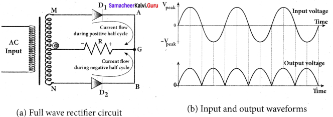
During positive half cycle:
When the positive half cycle of the ac input signal passes through the circuit, terminal M is positive, G is at zero potential and N is at negative potential. This forward biases diode D1 and reverse biases diode D2. Hence, being forward biased, diode D1 conducts and current flows along the path MD1 AGC. As a resul t, positive half cycle of the voltage appears across RL in the direction G to C.
During negative half cycle:
When the negative half cycle of the ac input signal passes through the circuit, terminal N is positive, G is at zero potential and M is at negative potential. This forward biases diode D2 and reverse biases diode D1. Hence, being forward biased, diode D2 conducts and current flows along the path ND2 BGC . As a result, negative half cycle of the voltage appears across RL in the same direction from G to C.
Hence in a full wave rectifier both positive and negative half cycles of the input signal pass through the circuit in the same direction as shown in figure (b). Though both positive and negative half cycles of ac input are rectified, the output is still pulsating in nature. The efficiency (η) of full wave rectifier is twice that of a half wave rectifier and is found to be 81.2 %. It is because both the positive and negative half cycles of the ac input source are rectified.
Question 5.
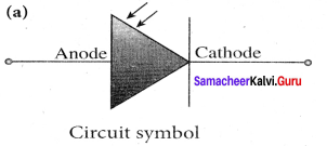
What is an LED? Give the principle of operation with a diagram.
Answer:
Light Emitting Diode (LED):
LED is a p – n junction diode which emits visible or invisible light when it is forward biased. Since, electrical energy is converted into light energy, this process is also called electroluminescence. The cross-sectional view of a commercial LED is shown in figure (b). it consists of a p-layer, n-layer and a substrate. A transparent window is used to allow light to travel in the desired direction. An external resistance in series with the biasing source is required to limit the forward current through the LED. In addition, it has two leads; anode and cathode:
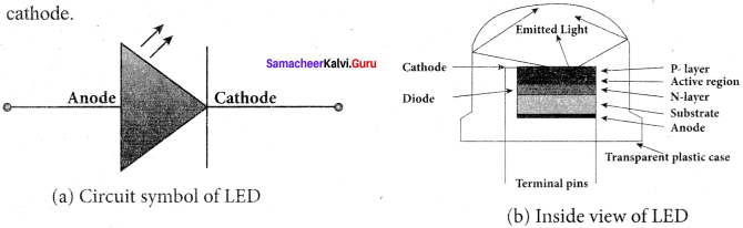
When the p – n junction is forward biased, the conduction band electrons on n-side and valence band holes on p-side diffuse across the junction. When they cross the junction, they become excess minority carriers (electrons in p-side and holes in n-side).
These excess minority carriers recombine with oppositely charged majority carriers in the respective regions, i.e. the electrons in the conduction band recombine with holes in the valence band as shown in the figure (c). During recombination process, energy is released in the form of light (radiative) or heat (non-radiative). For radiative recombination, a photon of energy hυ is emitted.
For non-radiative recombination, energy is liberated in the form of heat. The colour of the light is determined by the energy band gap of the material. Therefore, LEDs are available in a wide range of colours such as blue (SiC), green (AlGaP) and red (GaAsP). Now a days, LED which emits white light (GalnN) is also available.
Question 6.
Write notes on Photodiode?
Answer:
Photodiodes:
A p-n junction diode which converts an optical signal into electric current is known as photodiode. Thus, the operation of photodiode is exactly opposite to that of an LED. Photo diode words in reverse bias. Its circuit symbol is shown in figure (a). The direction of arrows indicates that the light is incident on the photo diode.
The device consists of a p – n junction semiconductor made of photosensitive material kept safely inside a plastic case. It has a small transparent window that allows light to be incident on the p – n junction. Photodiodes can generate current when the p – n junction is exposed to light and hence are called as light sensors.
When a photon of sufficient energy (hυ) strikes the depletion region of the diode, some of the valence band electrons are elevated into conduction band, in turn holes are developed in the valence band. This creates electron – hole pairs. The amount of electron – hole pairs generated depends on the intensity of light incident on the p-n junction. These electrons and holes are swept across the p-n junction by the electric field created by reverse voltage before recombination takes place. Thus, holes move towards the n-side and electrons towards the p-side.
When the external circuit is made, the electrons flow through the external circuit and constitute the photocurrent. When the incident light is zero, there exists a reverse current which is negligible. This reverse current in the absence of any incident light is called dark current and is due to the thermally generated minority carriers.
Question 7.
Explain the working principle of a solar cell. Mention its applications.
Answer:
Solar cell:
A solar cell, also known as photovoltaic cell, converts light energy directly into electricity or electric potential difference by photovoltaic effect. It is basically a p – n junction which generates emf when solar radiation falls on the p – n junction. A solar cell is of two types: p-type and n-type. Both types use a combination of p-type and n-type Silicon which together forms the p-n junction of the solar cell.
The difference is that p-type solar cells use p-type Silicon as the base with an ultra-thin layer of n-type Silicon as shown in Figure, while n-type solar cell uses the opposite combination. The other side of the p-Silicon is coated with metal which forms the back electrical contact. On top of the n-type Silicon, metal grid is deposited which acts as the front electrical contact. The top of the solar cell is coated with anti-reflection coating and toughened glass.
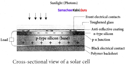
In a solar cell, electron-hole pairs are generated due to the absorption of light near the junction. Then the charge carriers are separated due to the electric field of the depletion region. Electrons move towards n-type Silicon and holes move towards p-type Silicon layer. The electrons reaching the n-side are collected by the front contact and holes reaching p-side are collected by the back electrical contact.
Thus a potential difference is developed across solar cell. When an external load is connected to the solar cell, photocurrent flows through the load. Many solar cells are connected together either in series or in parallel combination to form solar panel or module. Many solar panels are connected with each other to form solar arrays. For high power applications, solar panels and solar arrays are used.
Applications:
- Solar cells are widely used in calculators, watches, toys, portable power supplies, etc.
- Solar cells are used in satellites and space applications
- Solar panels are used to generate electricity.
![]()
Question 8.
Sketch the static characteristics of a common emitter transistor and bring out the essence of input and output characteristics.
Answer:
Static Characteristics of Transistor in Common Emitter Mode:
The know-how of certain parameters like the input resistance, output resistance, and current gain of a transistor are very important for the effective use of transistors in circuits. The circuit to study the static characteristics of an NPN transistor in the common emitter mode is given in figure.
The bias supply voltages VBB and VCC bias the base-emitter junction and collector- emitter junction respectively. The junction potential at the base-emitter is represented as VBE and the collector-emitter as VCE. The rheostats R1 and R2, are used to vary the base and collector currents respectively.
The static characteristics of the BJT are:
- Input characteristics
- Output characteristics
- Transfer characteristics
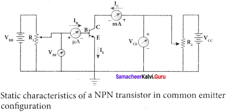
1. Input Characteristics:
Input Characteristics curves give the relationship between the base current (IB) and base to emitter voltage (VBE) at constant collector to emitter voltage (VCE) and are shown in figure. Initially, the collector to emitter voltage (VCE) is set to a particular voltage (above 0.7 V to reverse bias the junction). Then the base-emitter voltage (VBE) is increased in suitable steps and the corresponding base-current (IB) is recorded. A graph is plotted with VBE along the x-axis and IB along the y-axis. The procedure is repeated for different values of VCE.
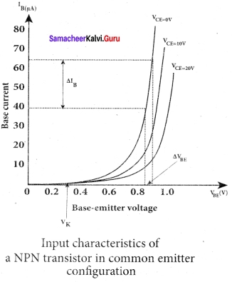
The following observations are made from the graph:
1. The curve looks like the forward characteristics of an ordinary p-n junction diode.
2. There exists a threshold voltage or knee voltage (Vk) below which the base current is very small. The value is 0.7 V for Silicon and 0.3 V for Germanium transistors. Beyond the knee voltage, the base current increases with the increase in base-emitter voltage.
3. It is also noted that the increase in the collector-emitter voltage decreases the base current. This shifts the curve outward. This is because the increase in collector-emitter voltage increases the width of the depletion region in turn, reduces the effective base width and thereby the base current.
Input resistance:
The ratio of the change in base-emitter voltage (∆VBE) to the change in base current (∆IB) at a constant collector-emitter voltage (VCE) is called the input resistance (Ri). The input resistance is not linear in the lower region of the curve.
Ri =\(\left(\frac{\Delta \mathrm{V}_{\mathrm{BE}}}{\Delta \mathrm{I}_{\mathrm{B}}}\right)_{\mathrm{V}_{\mathrm{CB}}}\)
The input resistance is high for a transistor in common emitter configuration. Output Characteristics:
The output characteristics give the relationship between the variation in the collector current (∆IC) with respect to the variation in collector- emitter voltage (∆ VCE) at constant input current (IB) as shown in figure.
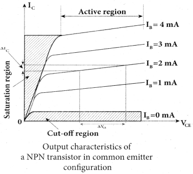
Initially, the base current (IB) is set to a particular value. Then collector- emitter voltage (VCE) is increased in suitable steps and the corresponding collector current (IC) is recorded. A graph is plotted with the VCE along the x-axis and IC along the y-axis.
This procedure is repeated for different values of IB, The four regions in are:
(i) Saturation region:
When VCE is increased above 0 V, the Ic increases rapidly to a saturation value almost independent of IB (Ohmic region, OA) called knee voltage. Transistors are always operated above this knee voltage.
(ii) Cut-off region:
A small collector current (IC) exists even after the base current (IB) is reduced to zero. This current is due to the presence of minority carriers across the collector-base junction and the surface leakage current (ICEO). This region is called as the cut-off region, because the main collector current is cut-off.
(iii) Active region:
In this region, the emitter-base junction is forward biased and the collector-base junction is reverse biased. The transistor in this region can be used for voltage, current and power amplification.
(iv) Breakdown region:
If the collector-emitter voltage (VCE) is increased beyond the rated value given by the manufacturer, the collector current (IC) increases enormously leading to the junction breakdown of the transistor. This avalanche breakdown can damage the transistor.
Output Resistance:
The ratio of the change in the collector-emitter voltage (∆VCE) to the corresponding change in the collector current (∆IC) at constant base current (IB ) is called output resistance (RO).
R0 =\(\left(\frac{\Delta \mathrm{V}_{\mathrm{CE}}}{\Delta \mathrm{I}_{\mathrm{C}}}\right)_{\mathrm{I}_{\mathrm{B}}}\)
The output resistance for transistor in common emitter configuration is very low.
Question 9.
Describe the function of a transistor as an amplifier with the neat circuit diagram. Sketch the input and output wave form.
Answer:
Transistor as an amplifier:
A transistor operating in the active region has the capability to amplify weak signals. Amplification is the process of increasing the signal strength (increase in the amplitude). If a large amplification is required, the transistors are cascaded with coupling elements like resistors, capacitors, and transformers which is called as multistage amplifiers.
Here, the amplification of an electrical signal is explained with a single stage transistor amplifier as shown in figure (a). Single stage indicates that the circuit consists of one transistor with the allied components. An NPN transistor is connected in the common emitter Configuration.
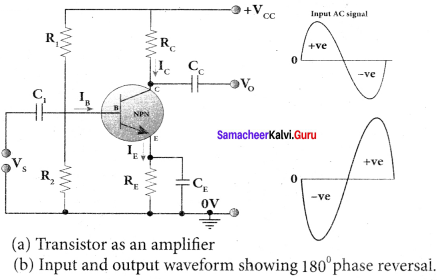
To start with, the Q point or the operating point of the transistor is fixed so as to get the maximum signal swing at the output (neither towards saturation point nor towards cut-off). A load resistance, RC is connected in series with the collector circuit to measure the output voltage. The capacitor C1 allows only the ac signal to pass through. The emitter bypass capacitor CE provides a low reactance path to the amplified ac signal. The coupling capacitor CC is used to couple one stage of the amplifier with the next stage while constructing multistage amplifiers. VS is the sinusoidal input signal source applied across the base-emitter.
Collector currrent ,Ic = IβB = [∴β=\(\frac { { I }_{ C } }{ { I }_{ B } } \)]
Applying Kirchhoff’s voltage law in the output loop, the collector-emitter voltage is given by
VCE = VCC – ICRC
Working of the amplifier:
1. During the positive half cycle:
Input signal (VS) increases the forward voltage across the emitter-base. As a result, the base current (IB) increases. Consequently, the collector current (IC) increases β times. This increases the voltage drop across RC which in turn decreases the collector-emitter voltage (VCE). Therefore, the input signal in the positive direction produces an amplified signal in the negative direction at the output. Hence, the output signal is reversed by 180° as shown in figure (b).
2. During the negative half cycle:
Input signal (Vs ) decreases the forward voltage across the emitter-base. As a result, base current (IB) decreases and in turn increases the collector current (IC). The increase in collector current (IC) decreases the potential drop across Rc and increases the collector-emitter voltage (VCE). Thus, the input signal in the negative direction produces an amplified signal in the positive direction at the output. Therefore, 180° phase reversal is observed during the negative half cycle of the input signal.
![]()
Question 10.
Transistor functions as a switch. Explain.
Answer:
The transistor in saturation and cut – off regions functions like an electronic switch that helps to turn ON or OFF a given circuit by a small control signal.
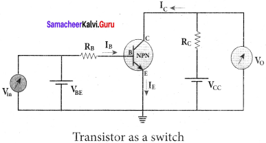
1. Presence of dc source at the input (saturation region):
When a high input voltage (Vin = +5V) is applied, the base current (IB) increases and in turn increases the collector current. The transistor will move into the saturation region (turned ON). The increase in collector current (IC) increases the voltage drop across Rc, thereby lowering the output voltage, close to zero. The transistor acts like a closed switch and is equivalent to ON condition.
2. Absence of dc source at the input (cut-off region):
A low input voltage (Vin = 0V), decreases the base current (IB) and in turn decreases the collector current (Ic). The transistor will move into the cut-off region (turned OFF). The decrease in collector current (Ic) decreases the drop across Rc, thereby increasing the output voltage, close to +5 V.
The transistor acts as an open switch which is considered as the OFF condition. It is manifested that, a high input gives a low output and a low input gives a high output. In addition, we can say that the output voltage is opposite to the applied input voltage. Therefore, a transistor can be used as an inverter in computer logic circuitry.
Question 11.
State Boolean laws. Elucidate how they are used to simplify Boolean expressions with suitable example.
Answer:
Law’s of Boolean Algebra: The NOT, OR and AND operations are \(\overline { A } \), A + B, A . B are the Boolean operations. The results of these operations can be summarised as:
Complement law
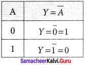
The complement law can be realised as ![]()
OR laws:
AND laws:
The Boolean operations obey the following laws.
Commutative laws
A+ B = B + A
A. B = B . A
Associative laws
A + (B + C) = (A + B) + C
A . (B . C) = (A .B) . C
Distributive laws
A( B + C) = AB + AC
A + BC = (A + B) (A + C)
The above laws are used to simplify complicated expressions and to simplify the logic circuitry.
![]()
Question 12.
State and prove De Morgan’s First and Second theorems.
Answer:
De Morgan’s First Theorem:
The first theorem states that the complement of the sum of two logical inputs is equal to the product of its complements.
Proof:
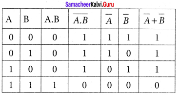
The Boolean equation for NOR gate is Y = \(\overline { A+B } \). The Boolean equation for a bubbled AND gate is Y = \(\overline { A } \). \(\overline { B } \) . Both cases generate same outputs for same inputs. It can be verified using the following truth table.
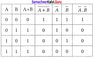
From the above truth table, we can conclude \(\overline { A+B } \) = \(\overline { A } \). \(\overline { B } \) . Thus De Morgan’s First Theorem is proved. It also says that a NOR gate is equal to a bubbled AND gate. The corresponding logic circuit diagram is shown in figure.
De Morgan’s Second Theorem:
The second theorem states that the complement of the product of two inputs is equal to the sum of its complements.
Proof:
The Boolean equation for NAND gate is Y = \(\overline { AB } \)
The Boolean equation for bubbled OR gate is Y = \(\overline { A } \) + \(\overline { B } \) . A and B are the inputs and Y is the output. The above two equations produces the same output for the same inputs. It can be verified by using the truth table.
From the above truth table we can conclude \(\overline { A.B } \) = \(\overline { A } \) + \(\overline { B } \). Thus De Morgan’s Second Theorem is proved. It also says, a NAND gate is equal to a bubbled OR gate. The corresponding logic circuit diagram is shown in figure.
Samacheer Kalvi 12th Physics Semiconductor Electronics Numerical Problems
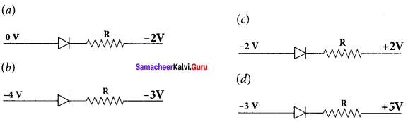
Question 1.
The given circuit has two ideal diodes connected as shown in figure below. Calculate the current flowing through the resistance R1.
Answer:
Diode D1 is reverse biased so, it will block the current and Diode D2 is forward biased, so it will pass the current.
Current in the circuit is
I = \(\frac { V }{ { R }_{ s } } \) = \(\frac { 10 }{ 2+2 }\) = \(\frac { 10 }{ 4 }\) = 2.5 a
I = 2.5 A
![]()
Question 2.
Four silicon diodes and a 10 resistor are connected as shown in figure below. Each diode has a resistance of 1Ω Find the current flows through the 18Ω resistor.
Answer:
Diodes D2 and D4 are forward biased while diodes D1 and D3 are reverse biased. Only current flowing through the closed loop is EADCBFE. Consider the applied voltage is 4V. For silicon diode, Barrier Voltage is 0.7V.
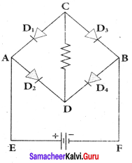
Net circuit Voltages = 4 – (0.7 + 0.7) = 4 1.4
V = 2.6 V
Total circuit resistance = 1 + 18 + 1
R = 20 Ω
∴ Circuit Current I = \(\frac { V }{ R }\) = \(\frac { 2.6 }{ 20 }\)
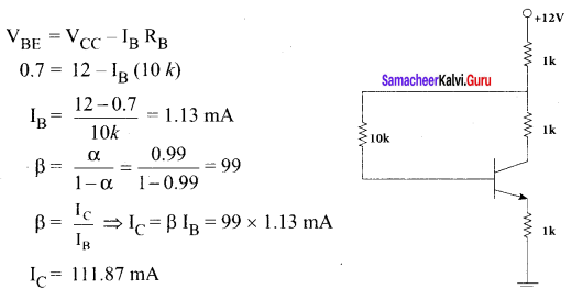
Question 3.
Assuming VCEsat = 0.2 V and β = 50, find the minimum base current (IB) required to drive the transistor given in the figure to saturation.
Solution:
![]()
Question 4.
A transistor having α =0.99 and VBE = 0.7V, is given in the circuit. Find the value of the collector current.
Solution:
Question 5.
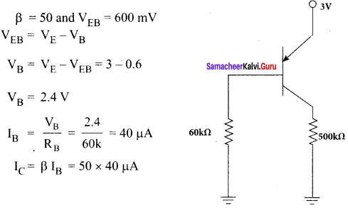
In the circuit shown in the figure, the BJT has a current gain (β) of 50. For an emitter – base voltage VEB = 600 mV, calculate the emitter – collector voltage VEC (in volts).
Solution:
Samacheer Kalvi 12th Physics Semiconductor Electronics Additional Questions
Samacheer Kalvi 12th Physics Semiconductor Electronics Multiple Choice Questions
Question 1.
The probability of electrons to be found in the conduction band of an intrinsic semiconductor at a finite temperature
(a) increase exponentially with increasing band gap
(b) decrease exponentially with increasing band gap
(c) decreases with increasing temperature
(d) is independent of the temperature and the band gap.
Answer:
(b) decrease exponentially with increasing band gap
Hint:
At a finite temperature, the probability of jumping an electron from valence band to conduction band decreases exponentially with the increasing band gap (Eg )
n = n0 e-Eg/kBT
Question 2.
The electrical conductivity of a semiconductor increase when electromagnetic radiation of wavelength shorter than 2480 nm is incident on it. The band gap (in eV) for the semiconductor is-
(a) 0.9
(b) 0.7
(c) 0.5
(d) 1.1.
Answer:
(c) 0.5
Hint:
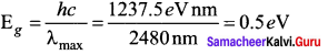
![]()
Question 3.
Which of the following statements is not true?
(a) The resistance of intrinsic semiconductor decreases with increase of temperature.
(b) Doping pure Si with trivalent impurities gives p-type semiconductors.
(c) The majority carriers in n-type semiconductors and holes
(d) Ap-n junction can act as a semiconductor diode.
Answer:
(c) The majority carriers in n-type semiconductors and holes
Hint:
The majority charge carriers in n-type semiconductors are electrons not holes. Only option (c) is not true.
Question 4.
Holes are charge carrier in
(a) intrinsic semiconductors
(b) ionic solids
(c) p-type semiconductor
(d) metals.
Answer:
(a) intrinsic semiconductors
Hint:
(a) In intrinsic semiconductor, nh = ne
(b) In P-type semiconductor, nh >> ne
Question 5.
A transistor is used in the common emitter mode as an amplifier. Then
(a) the base – emitter junction is forward – biased
(b) the base – emitter junction is reverse – biased
(c) the input signal is connected in series with the voltage applied to bias the base – emitter junction
(d) the input signal is connected in series with the voltage applied to bias the base – collector junction.
Answer:
(c) the input signal is connected in series with the voltage applied to bias the base – emitter junction
Hint:
In CE – transistor amplifier, the base – emitter junction is forward bias and the input signal is connected in series with the base – emitter battery.
![]()
Question 6.
The energy band gap is maximum in-
(a) metals
(b) superconductors
(c) insulators
(d) semiconductors.
Answer:
(c) insulators
Hint:
The band gap is maximum in insulators.
Question 7.
At absolute zero, Si acts as-
(a) non – metal
(b) metal
(c) insulator
(d) none of these.
Answer:
(c) insulator
Hint:
At absolute zero, Si acts as an insulator due to the absence of free electrons in the conduction band.
Question 8.
Apiece of copper and another of germanium are cooled from room temperature to 77 K. The resistance of
(a) each of these decreases
(b) copper strip increases and that of germanium decreases
(c) copper strip decreases and that of germanium increases
(d) each of these increases.
Answer:
(c) copper strip decreases and that of germanium increases
Hint:
With the decrease of temperature, the resistance of copper (a metallic conductor) decreased while that of germanium (a semiconductor) increases.
Question 9.
In the middle of the depletion layer of reverse biased p – n junction, the-
(a) electric field is zero
(b) potential is zero
(c) potential is maximum
(d) electric field is maximum.
Answer:
(a) electric field is zero
Hint:
When a p – n junction is reverse biased, the width of the depletion layer becomes large and so the electric field (E = v/d) becomes very small, nearly zero.
Question 10.
In a full wave rectifier circuit operating from 50 Hz mains, frequency, the fundamental frequency in the ripple would be-
(a) 50 Hz
(b) 25 Hz
(c) 100 Hz
(d) 70.7 Hz.
Answer:
(c) 100 Hz
Hint:
The frequency of the ripple in the output of a fullwave rectifier is twice the frequency of the a.c. input. Hence, it is 100 Hz.
![]()
Question 11.
The part of a transistor, which is heavily doped to produce a large number of majority carriers is called?
(a) emitter
(b) base
(c) collector
(d) any one out of emitter, base and collector.
Answer:
(a) emitter
Hint:
Emitter of a transistor is heavily doped so as to act as source of majority charge carriers.
Question 12.
When n – p – n transistor is used as an amplifier, then-
(a) electrons move from base to collector
(b) holes move from emitter to base
(c) electrons move from collector to base
(d) holes move from base to emitter.
Answer:
(a) electrons move from base to collector
Hint:
When n – p – n transistor is in operation, the majority charge carriers, i.e., electrons move from emitter to base and then to collector.
Question 13.
In a common – base amplifier, the phase difference between the input signal voltage and the output voltage (across collector and base) is
(a) 0
(b) π/4
(c) π/2
(d) π.
Answer:
(a) 0
Hint:
In a common – base amplifier, the input and output voltages are in the same phase.
Question 14.
In a common – base mode of a transistor, the collector current is 5.488 mA for an emitter current of 5.60 A. The value of the base current amplification factor (β) will be-
(a) 49
(b) 50
(c) 51
(d) 48.
Answer:
(a) 49
Hint:
β = \(\frac { { I }_{ C } }{ { I }_{ B } } \) = \(\frac { 5.488 }{ 0.112 }\) = 49.
Question 15.
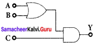
In the circuit below, A and B represent two inputs and C represents the output. The circuit represents
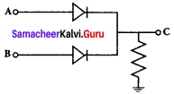
(a) OR gate
(b) NOR gate
(c) AND gate
(d) NAND gate.
Answer:
(a) OR gate
Hint:
The given circuit represents an OR gate, when either A or B or both inputs are high, the output C is high.
![]()
Question 16.
In a fee lattice structure, what is the effective number of atoms?
(a) 4
(b) 3
(c) 2
(d) 1.
Answer:
(a) 4
Hint:
N = \(\frac { { N }_{ C } }{ 8 } \) + \(\frac { { N }_{ F } }{ 2 } \) = \(\frac { 8 }{ 8 }\) + \(\frac { 6 }{ 2 }\) = 4.
Question 17.
Monoclinic crystal lattice has dimensions-
(a) α = β = γ
(b) α = β = 90°, γ ≠ 90°
(e) α ≠ β ≠ γ
(d) none of these.
Answer:
(b) α = β = 90°, γ ≠ 90°
Hint:
For a monoclinic crystal, α ≠ β ≠ c and α = β = 90°≠ γ.
Question 18.
In insulators?
(a) valence band is partially filled
(b) conduction band is partially filled with electrons
(c) conduction band is filled with electrons and valence band is empty
(d) conduction band is empty and valence band is completely filled with electrons.
Answer:
(d) conduction band is empty and valence band is completely filled with electrons.
Hint:
In insulators, the conduction band is empty and valence band is completely filled with electrons.
![]()
Question 19.
The valence band and conduction band of a solid overlap at low temperature, the solid may be-
(a) a metal
(b) a semiconductor
(c) an insulator
(d) none of these.
Answer:
(a) a metal
Hint:
In metals, the valence band and conduction band may overlap at low temperature.
Question 20.
If germanium is dopped with arsenic, that will result in-
(a) n-type semiconductor
(b) p-type semiconductor
(c) intrinsic semiconductor
(d) none of these.
Answer:
(a) n-type semiconductor
Hint:
Arsenic is pentavalent. Its doping with germanium results in n-type semiconductor.
Question 21.
n-type semiconductor is
(a) positive charged
(b) negatively charged
(c) neutral
(d) positive or negative depending upon doping material.
Answer:
(c) neutral
Hint:
Semiconductors maintain their electrical neutrality even after doping.
![]()
Question 22.
To a germanium ciystal equal number of aluminium and indium atoms are added. Then
(a) it remains an intrinsic semiconductor
(b) it becomes an n-type semiconductor
(c) it becomes a p-type semiconductor
(d) it becomes an insulator.
Answer:
(c) it becomes a p-type semiconductor
Hint:
Both A1 and In are trivalent atoms. Their doping in germanium results in a p-type semiconductor.
Question 23.
The dominant contribution to current comes from holes in case of-
(a) metals
(b) intrinsic semiconductors
(c) p-type extrinsic semiconductors
(d) n-type extrinsic semiconductors.
Answer:
(c) p-type extrinsic semiconductors
Hint:
Holes are the majority charge carriers in p-type extrinsic semiconductors.
Question 24.
For a heavily doped n-type semiconductor, fermi – level lies-
(a) a little below the conduction band
(b) a little above the valence band
(c) a little inside the valence band
(d) at the centre of the band gap.
Answer:
(a) a little below the conduction band
Hint:
For a heavily doped n-type semiconductor, the fermi level lies slightly below the bottom of the conduction band.
![]()
Question 25.
The coordination number for a bcc crystal is-
(a) 4
(b) 8
(c) 12
(d) 6.
Answer:
(b) 8
Hint:
The eight comer atoms of the unit cell are close neighbourers of the atom at the body centre.
Question 26.
If the forward voltage in a diode is increased the width of the depletion region-
(a) increases
(b) decreases
(c) fluctuates
(d) no change.
Answer:
(b) decreases
Hint:
If the forward voltage in a diode is increased, the width of depletion region decreases.
Question 27.
In order to rectify an alternating current one uses a-
(a) thermocouple
(b) diode
(c) triode
(d) transistor.
Answer:
(b) diode
Hint:
A diode is used to rectify an alternating current.
Question 28.
Why is there sudden increase in current in zener diode?
(a) due to rupture of bonds
(b) resistance of depletion layer becomes less
(c) due to high doping
(d) none of the above.
Answer:
(a) due to rupture of bonds
Hint:
The sudden increase in current in a zener diode is due to the rupture of many covalent bonds.
![]()
Question 29.
In a transistor
(a) there is 1 p – n junction
(b) there are 2 p – n junction
(c) there are 3 p – n junction
(d) none of the above.
Answer:
(b) there are 2 p – n junction
Hint:
A transistor is like a combination of two p-n junctions placed back to back.
Question 30.
Let ie, ic and ib represent emitter current, collector current and the base current of a transistor, then
(a) ic > ie
(b) ib > ic
(c) ib < ic
(d) ie > ic
Answer:
(d) ie > ic
Hint:
As ie = ic + ib
∴ ii >c
Question 31.
In common – emitter amplifier the ratio \(\frac { { I }_{ C } }{ { I }_{ E } } \) is 0.98. The current gain will be
(a) 4.9
(b) 7.8
(c) 49
(d) 78.
Answer:
(c) 49
Hint:
\(\frac { α }{ 1-α } \) = \(\frac { 0.98 }{ 1-0.98 } \) = \(\frac { 0.98 }{ 0.02 } \) = 49
Question 32.
The gate for which output is high, if atleast one input is low?
(a) NAND
(b) NOR
(c) AND
(d) OR.
Answer:
(a) NAND
Hint:
The output of a NAND gate is high, if atleast one input is low.
![]()
Question 33.
An oscillator is nothing but an amplifier with-
(a) positive feedback
(b) large gain
(c) no feedback
(d) negative feedback.
Answer:
(a) positive feedback
Hint:
When a transistor is used as an amplifier with positive feedback, it works as an oscillator.
Question 34.
Crystalline solid are?
(a) anisotropic
(b) isotropic
(c) amporphus
(d) none of these.
Answer:
(a) anisotropic
Hint:
Crystalline solids are anisotropic as they show different physical properties along different directions.
Question 35.
Which of the following is an amorphous solid?
(a) Glass
(b) Diamond
(c) Salt
(d) Sugar.
Answer:
(a) Glass
Question 36.
Energy required to break one band in DNA is
(a) ≈ 1 eV
(b) ≈ 0.1 eV
(c) ≈ 0.01 eV
(d) ≈ 2.1 eV.
Answer:
(a) ≈ 1 eV
Hint:
The bond strength in DNA is nearly 1 eV.
Question 37.
An intrinsic semiconductor, at the absolute zero temperature, behaves like a/an?
(a) insulator
(b) superconductor
(c) n-type semiconductor
(d) p-type semiconductor.
Answer:
(a) insulator
Hint:
At the absolute zero temperature, an intrinsic semiconductor behaves like an insulator.
Question 38.
In a semiconducting material the mobilities of electrons and holes are µe and µh respectively. Which of the following is true?
(a) µe > µh
(b)µe < µh
(c) µe = µh
(d)µe < 0 ; µh > 0.
Answer:
(a) µe > µh
Hint:
The mobility of an electron in the conduction is more than the mobility of a hole in the valence band.
![]()
Question 39.
In a pure semiconductor crystal, if current flows due to breakage of crystal bonds, then the semiconductor is called
(a) acceptor
(b) donor
(c) intrinsic semiconductor
(d) extrinsic semiconductor.
Answer:
(c) intrinsic semiconductor
Hint:
Pure semiconductors are called intrinsic semiconductors.
Question 40.
Which of the following, when added as an impurity into the silicon, produces n-type semiconductor?
(a) phosphorous
(b) aluminium
(c) magnesium
(d) both (b) and (c).
Answer:
(a) phosphorous
Hint:
As phosphorous is pentavalent, it produces n-type semiconductor when added to silicon.
Question 41.
In n-type semiconductors, majority charge carriers are
(a) holes
(b) protons
(c) neutrons
(d) electrons.
Answer:
(d) electrons
Question 42.
In p-type semiconductor,
(a) major current carrier are electrons
(b) major carrier are mobile negative ions
(c) major carrier are mobile holes
(d) the number of mobile holes exceeds the number of acceptor atoms.
Answer:
(c) major carrier are mobile holes
Hint:
In p-type semiconductors, holes are the majority charge carriers.
Question 43.
The potential barrier in the depletion layer is due to-
(a) ions
(b) holes
(c) electrons
(d) forbidden band.
Answer:
(a) ions
Hint:
The potential barrier in the depletion layer is due to the presence of immobile ions.
Question 44.
When a p-n diode is reverse biased, then
(a) no current flows
(b) the depletion region is increased
(c) the depletion region is reduced
(d) the height of the potential barrier is reduced.
Answer:
(b) the depletion region is increased
Hint:
When a p-n junction is reverse biased, its depletion region is widened.
![]()
Question 45.
If a p-n diode is reverse biased, then the resistance measured by an ohm meter, will be
(a) zero
(b) low
(c) high
(d) infinite.
Answer:
(c) high
Hint:
When a p-n diode is reverse biased, it offers a high resistance.
Question 46.
Diode is used as an/a?
(a) oscillator
(b) amplifier
(c) rectifier
(d) modulator.
Answer:
(c) rectifier
Question 47.
In the half wave rectifier circuit operating from 50 Hz main frequency, the fundamental frequency in the ripple would be-
(a) 25 Hz
(b) 50 Hz
(c) 70.7 Hz
(d) 100 Hz
Answer:
(b) 50 Hz.
Hint:
In a half wave rectifier, fundamental frequency in the ripple = Input frequency = 50 Hz.
![]()
Question 48.
Zener diode acts as a/an?
(a) oscillator
(b) regulator
(c) rectifier
(d) filter.
Answer:
(b) regulator
Question 49.
A transistor is a/an?
(a) chip
(b) insulator
(c) semiconductor
(d) metal.
Answer:
(c) semiconductor
Question 50.
The minimum potential difference between the base and emitter required to switch a silicon transistor ON is approximately.
(a) IV
(b) 3V
(c) 5V
(d) 4.2 V.
Answer:
(a) IV
Hint:
For switching on a silicon transistor, (VBE)min ≈ 1V.
Question 51.
When n-p-n transistor is used as an amplifier, then
(a) holes moves from emitter
(b) electrons move from base to collector
(c) holes move from base to emitter
(d) electrons move from collector to base.
Answer:
(b) electrons move from base to collector
Question 52.
The current gain for a transistor working as common base amplifier is 0.96. If the emitter current is 7.2 mA, then the base current is-
(a) 0.29 mA
(b) 0.35 mA
(c) 0.39 mA
(d) 0.43 mA.
Answer:
(a) 0.29 mA
Hint:
α = \(\frac { { I }_{ C } }{ { I }_{ E } } \) (or) 0.96 = \(\frac { { I }_{ C } }{ 7.2mA} \)
IC = 0.96 x 7.2 = 6.91 mA
IB = IC – IE = 7.2 – 6.91 =0.29 mA.
![]()
Question 53.
Consider an n-p-n transistor amplifier in common – emitter configuration. The current gain of the transistor is 100. If the collector current changes by 1 mA, what will be the change in emitter current?
(a) 1.1 mA
(b) 1.01 mA
(c) 0.01 mA
(d) 10 mA.
Answer:
(b) 1.01 mA
Hint:
β = \(\frac { { \triangle I }_{ C } }{ { \triangle I }_{ E } } \) ∴ ∆IB = \(\frac { { \triangle I }_{ C } }{ β } \) = \(\frac { 1mA }{ β }\) = 0.01 mA
∆IE= ∆IB + ∆IC = 0.01 + 1 = 1.01 mA.
Question 54.
An amplifier has voltage gain = 1000. The voltage gain (in dB) is-
(a) 30 dB
(b) 60 dB
(c) 3 dB
(d) 20 dB.
Answer:
(b) 60 dB
Hint:
Voltage gain in dB = 20 log10 Av= 20 log10 (1000) = 20 x 3 = 60 dB.
Question 55.
Boolean algebra is essentially based on-
(a) logic
(b) truth
(c) numbers
(d) symbol.
Answer:
(a) logic
Question 56.
The number (0) zero is required for-
(a) transistor
(b) abacus
(c) computer
(d) calculator.
Answer:
(c) computer
Hint:
A computer work on binary digits 0 and 1.
![]()
Question 57.
Which of the following logic gates in a universal gate?
(a) OR
(b) NOT
(c) AND
(d) NAND.
Answer:
(d) NAND.
Hint:
NAND gate is a universal gate because its repeated use can give all basic gates like OR, AND and NOT gates.
Question 58.
Which of the following is the weakest kind of the bonding in solids?
(a) Ionic
(b) Metallic
(c) Van der waals
(d) Covalent.
Answer:
(c) Van der waals
Question 59.
The cations and anions are arranged in alternate form in-
(a) metallic crystal
(b) ionic crystal semi – conductor
(c) covalent crystal
(d) crystal.
Answer:
(b) ionic crystal semi – conductor
![]()
Question 60.
Diamond is very hard because-
(a) it is covalent solid
(b) it has large cohesive energy
(c) high melting point
(d) insoluble in all solvents.
Answer:
(b) it has large cohesive energy
Question 61.
Number of atoms per unit cell in bcc lattice is-
(a) 9
(b) 4
(c) 2
(d) 1.
Answer:
(c) 2
Hint:
N = NB + \(\frac { { N }_{ C } }{ 8 } \) = 1 + \(\frac { 8 }{ 8 }\) = 2.
Question 62.
At absolute zero, Si acts as?
(a) non metal
(b) metal
(c) 2
(d) 1.
Answer:
(c) 2
Hint:
At absolute zero, Si acts as an insulator because it has no free electrons in the conduction band.
Question 63.
Which of the following, when added as an impurity into the silicon produces n-type semi – conductor?
(a) B
(b) AL
(c) P
(d) Mg.
Answer:
(c) P
Hint:
Only P is a pentavalent impurity atom,its doping with germanium produces a p-types semi – conductor.
![]()
Question 64.
To obtain a p-type germanium semiconductor, it must be doped with-
(a) indium
(b) phosphorus
(c) arsenic
(d) antimony.
Answer:
(a) indium
Hint:
Only In is a trivalent impurity atom, its doping with germanium produces a p-type semi-conductor.
Question 65.
When arsenic is added as an impurity to silicon, the resulting material is-
(a) n-type conductor
(b) n-type semiconductor
(c) P – type semiconductor
(d) none of these.
Answer:
(b) n-type semiconductor
Hint:
When pentavalent arsenic is doped to silicon, it forms n-type semi – conductor.
Question 66.
In a p-type semiconductor, the majority carriers of current are-
(a) protons
(b) electrons
(c) holes
(d) neutrons.
Answer:
(c) holes
Question 67.
The depletion layer in the p – n junction region is caused by-
(a) drift of holes
(b) diffusion of charge carriers
(c) migration of impurity ions
(d) drift of electrons.
Answer:
(b) diffusion of charge carriers
Hint:
The depletion layer in the p-n junction region is caused by diffusion of charge carriers.
Question 68.
In the depletion region of an unbiased p – n junction diode, there are-
(a) holes
(b) mobile ions
(c) electrons
(d) immobile ions.
Answer:
(d) immobile ions.
Hint:
The depletion layer consists of immobile ions.
Question 69.
In forward bias, the width of potential barrier in a p – n junction adiode.
(a) remain constant
(b) decreases
(c) increases
(d) first (a) then (b).
Answer:
(b) decreases
![]()
Question 70.
Reverse bias applied to a junction diode-
(a) lowers the potential barrier
(b) raises the potential barrier
(c) increases the majority carrier current
(d) increases the minority carrier current.
Answer:
(b) raises the potential barrier
Question 71.
Barrier potential of a p – n junction diode does not depend on-
(a) diode design
(b) temperature
(c) forward bias
(d) doping density.
Answer:
(a) diode design
Hint:
Barrier potential depends upon temperature, doping density and forward biasing.
Question 72.
The peak voltage in the output of a half wave diode rectifier fed with a sinusoidal signal without filter is 10 V. The d.c component of the output voltage is-
(a) \(\frac { 10 }{ \sqrt { 2V } } \)
(b) \(\frac { 10 }{ πV }\)
(c) 10v
(d) \(\frac { 20 }{ πV }\).
Answer:
(b) \(\frac { 10 }{ πV }\)
Hint:
Vdc = Vm = \(\frac { { V }_{ 0 } }{ π } \) = \(\frac { 10 }{ π }\) V.
Question 73.
A p-n junction diode can be used as-
(a) condenser
(b) regulator
(c) amplifier
(d) rectifier.
Answer:
(d) rectifier.
Question 74.
Zener diode is used for-
(a) amplification
(b) rectification
(c) stabilisation
(d) producing oscillations in an oscillator.
Answer:
(d) producing oscillations in an oscillator.
Hint:
Zener diode can be used for stabilisation of voltage.
![]()
Question 75.
When n-p-n transistor is used as an amplifier, then
(a) electrons move from collector to base
(b) holes move from base to emitter
(c) electrons move from base to collector
(d) electrons move from emitter to base
Answer:
(c) electrons move from base to collector
Hint:
When n-p-n transistor is used an amplifier, the majority carrier electrons move from base to collector.
Question 76.
The correct relationship between the two current gains a and P in a transistor is-
(a) α = \(\frac { β }{ 1+β }\)
(b) α = \(\frac { 1+β }{ β }\)
(c) β = \(\frac { α }{ 1+α }\)
(d) β = \(\frac { α }{ α-1 }\).
Answer:
(a) α = \(\frac { β }{ 1+β }\)
Hint:
β = \(\frac { α }{ 1+α }\) (or) β – βα = α ; α = \(\frac { β }{ 1+β }\).
Question 77.
The correct relation for a, P for a transistor is-
(a) β = \(\frac { 1-α }{ α }\)
(b) β = \(\frac { α }{ 1-α }\)
(c) α = \(\frac { β-1 }{ β }\)
(d) αβ = 1.
Answer:
(b) β = \(\frac { α }{ 1-α }\)
Question 78.
For a common base circuit if \(\frac {{ I }_{C}}{ { I }_{E} }\) = 0.98, then current gain for common emitter circuit will be-
(a) 49
(b) 98
(c) 4.9
(d) 25.5.
Answer:
(a) 49
Hint:
Here \(\frac {{ I }_{C}}{ { I }_{E} }\) = α = 0.98 ; β = \(\frac { α }{ 1-α }\) = \(\frac { 0.98 }{ 1-0.98 }\) = 49.
Question 79.
Radio waves of constant amplitude can be generated with-
(a) FET
(b) filter
(c) rectifier
(d) oscillator.
Answer:
(d) oscillator.
Question 80.
An oscillator is an amplifier with-
(a) a large gain
(b) negative feedback
(c) positive feedback
(d) no feedback.
Answer:
(c) positive feedback
![]()
Question 81.
The output of OR gate is 1
(a) if both inputs are zero
(b) if either or both inputs are 1
(c) only if both inputs are 1
(d) if either input is zero.
Answer:
(b) if either or both inputs are 1
Question 82.
The device that can act as a complete electronic circuit is-
(a) junction diode
(b) integrated circuit
(c) junction transistor
(d) zener diode.
Answer:
(b) integrated circuit
Question 83.
At absolute zero temperature, a semiconductor acts as a/an.
(a) dielectric
(b) conductor
(c) insulator
(d) none of these.
Answer:
(c) insulator
Question 84.
At which temperature, a pure semiconductor behave slightly as a conductor?
(a) low temperature
(b) room temperature
(c) high temperature
(d) both (a) and (b).
Answer:
(b) room temperature
![]()
Question 85.
In germanium crystal, the forbidden energy gap in joule is.
(a) 1.6 x 10⁻¹⁹
(b) zero
(c) 1.12 x 10⁻¹⁹
(d) 1.76 x 10⁻¹⁹
Answer:
(c) 1.12 x 10⁻¹⁹
Hint:
For a germanium crystal,
Eg = 0.7 eV = 0.7 x 1.6 x 10-19 J = 1.12 x 10⁻¹⁹ J.
Question 86.
In a p-type semiconductor, germanium is doped with.
(a) gallium
(b) boron
(c) aluminium
(d) all of these
Answer:
(d) all of these
Hint:
Ga, B and A1 are all trivalent atoms, they produce p-type semiconductor.
Question 87.
The major carrier of current in a p-type semiconductor will be.
(a) neutrons
(b) protons
(c) electrons
(d) holes.
Answer:
(d) holes.
Hint:
Holes are the major carriers of current in a p-type semiconductor.
![]()
Question 88.
Rectification is the process of conversion of
(a) a.c into d.c
(b) low a.c into high a.c
(c) d.c into a.c
(d) low d.c into high d.c
Answer:
(a) a.c into d.c
Question 89.
Which type of gate is represented by the given figure?
(a) NAND
(b) NOT
(c) AND
(d) OR.
Answer:
(b) NOT
Hint:
When both the inputs of a NAND gate are joined, it functions as a NOT gate.
Question 90.
Which of the following gates can be served as a building block for any digital circuit?
(a) OR
(b) NOT
(c) AND
(d) NAND.
Answer:
(d) NAND.
Hint:
A NAND gate is a universal gate.
Samacheer Kalvi 12th Physics Semiconductor Electronics Short Answer Questions
Question 1.
What are passive and active components.
Answer:
Passive components:
Components that cannot generate power in a circuit.
Active components:
components that can generate power in a circuit.
![]()
Question 2.
What are energy band?
Answer:
The band of very large number of closely spaced energy levels in a very small energy range is known as energy band.
Question 3.
What are valence band, conduction band and forbidden energy gap.
Answer:
The energy band formed due to the valence orbitals is called valence band and that formed due to the unoccupied orbitals is called the conduction band. The energy gap between the valence band and the conduction band is called forbidden energy gap.
Question 4.
What are intrinsic semiconductor?
Answer:
A semiconductor in its pure form without impurity is called an intrinsic semiconductor. In intrinsic semiconductors, the number of electrons in the conduction band is equal to the number of holes in the valence band.
Question 5.
What are extrinsic semiconductor?
Answer:
An extrinsic semiconductor is a semiconductor doped by a specific impurity which is able to deeply modify its electrical properties, making it suitable for electronic applications (diodes, transistors etc.) or optoelectronic applications (light emitters and detectors).
![]()
Question 6.
What are holes?
Answer:
The vacancy or absense of an electron in the bond of a covalently bonded crystal is called a hole.
Question 7.
What is meant by biasing and bias voltage?
Answer:
Biasing means providing external energy to charge carriers to overcome the barrier potential and make them move in a particular direction. The external voltage applied to the p-n junction is called bias voltage.
Question 8.
What are called forward bias and reverse bias?
Answer:
- If the positive terminal of the external voltage source is connected to the p-side and the negative terminal to the n-side, it is called forward bias.
- If the positive terminal of the battery is connected to the n-side and the negative potential to the p-side, the junction is said to be reverse biased.
![]()
Question 9.
Define knee voltage or threshold voltage or cut-in voltage.
Answer:
At room temperature, a potential difference equal to the barrier potential is required before a reasonable forward current starts flowing across the diode. This voltage is known as threshold voltage or cut-in voltage or knee voltage (Vth).
Question 10.
What is a Rectification?
Answer:
Rectification is the process of converting alternating current into direct current is called rectification.
Question 11.
Define – Efficiency of rectifier.
Answer:
Efficiency (η) is the ratio of the output dc power to the ac input power supplied to the circuit.
Question 12.
What is meant by zener effect?
Answer:
The electric field is strong enough to break or rupture the covalent bonds in the lattice and thereby generating electron-hole pairs. This effect is called Zener effect.
Question 13.
What is a zener diode?
Answer:
A junction diode specially designed to operate only in the reverse breakdown region continuously (without getting damaged) is called a zener diode.
![]()
Question 14.
Write down the applications of zener diode.
Answer:
The zener diode can be used as:
- Voltage regulators
- Peak clippers
- Calibrating voltages
- Provide fixed reference voltage in a network for biasing
- Meter protection against damage from accidental application of excessive voltage.
Question 15.
What is peak inverse voltage (PIV)?
Answer:
The maximum reverse bias that can be applied before entering into the Zener region is called the Peak inverse voltage.
Question 16.
What is Optoelectronic devices?
Answer:
Optoelectronics deals with devices which convert electrical energy into light and light into electrical energy through semiconductors.
![]()
Question 17.
Write down the applications of LED’s?
Answer:
- Indicator lamps on the front panel of the scientific and laboratory equipments.
- Seven-segment displays.
- Traffic signals, exit signs, emergency vehicle lighting etc.
- Industrial process control, position encoders, bar graph readers.
Question 18.
Write down the applications of photodiodes?
Answer:
- Alarm system
- Count items on a conveyer belt
- Photoconductors
- Compact disc players, smoke detectors
- Medical applications such as detectors for computed tomography etc.
Question 19.
Write down the applications of solar cell.
Answer:
- Solar cells are widely used in calculators, watches, toys, portable power supplies, etc.
- Solar cells are used in satellites and space applications
- Solar panels are used to generate electricity.
Question 20.
What is a solar cell.
Answer:
A solar cell, also known as photovoltaic cell, converts light energy directly into electricity or electric potential difference by photovoltaic effect.
![]()
Question 21.
Write down the applications of Oscillators.
Answer:
Applications of oscillators:
- to generate a periodic sinusoidal or non sinusoidal wave forms.
- to generate RF carriers.
- to generate audio tones
- to generate clock signal in digital circuits.
- as sweep circuits in TV sets and CRO.
Question 22.
Write down concept of Barkhausen conditions for sustained oscillations.
Answer:
Barkhausen conditions for sustained oscillations
The following condition called Barkhausen conditions should be satisfied for sustained oscillations in the oscillator.
- The loop phase shift must be 0° or integral multiples of 2π.
- The loop gain must be unity. |Aβ| = 1
Here; A → Voltage gain of the amplifier,
b → feedback ratio; (fraction of the output that is fed back to the input)
Samacheer Kalvi 12th Physics Semiconductor Electronics Long Answer Questions
Question 1.
Explain the classification of materials.
Answer:
Insulators:
The valence band and the conduction band are separated by a large energy gap. The forbidden energy gap is approximately 6 eV in insulators. The gap is very large that electrons from valence band cannot move into conduction band even on the application of strong external electric field or the increase in temperature. Therefore, the electrical conduction is not possible as the free electrons are almost nil and hence these materials are called insulators. Its resistivity is in the range of 1011 – 1019 Ωm.
Metals:
In metals, the valence band and conduction band overlap. Hence, electrons can move freely into the conduction band which results in a large number of free electrons in the conduction band. Therefore, conduction becomes possible even at low temperatures. The application of electric field provides sufficient energy to the electrons to drift in a particular direction to constitute a current. For metals, the resistivity value lies between 10-2 and 10-8 Ωm.
Semiconductors:
In semiconductors, there exists a narrow forbidden energy gap (Eg < 3 eV ) between the valence band and the conduction band. At a finite temperature, thermal agitations in the solid can break the covalent bond between the atoms (covalent bond is formed due to the sharing of electrons to attain stable electronic configuration). This releases some electrons from valence band to conduction band. Since free electrons are small in number, the conductivity of the semiconductors is not as high as that of the conductors. The resistivity value of semiconductors is from 10-5 to 106 Ωm.
![]()
Question 2.
Explain zener diode as a voltage regulator.
Answer:
Zener diode as a voltage regulator:
A Zener diode working in the breakdown region can serve as a voltage regulator. It maintains a constant output voltage even when input voltage Vi or load current IL varies. Here, in this circuit the input voltage Vi is regulated at a constant voltage, Vz (Zener voltage) at the output represented as V0 using a Zener diode. The output voltage is maintained constant as long as the input voltage does not fall belowVz.
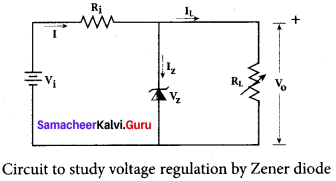
When the potential developed across the diode is greater than Vz ,the diode moves into the Zener breakdown region. It conducts and draws relatively large current through the series resistance Ri. The total current I passing through Ri equals the sum of diode current Iz and load current IL (I = Iz + IL) It is to be noted that the total current is always less than the maximum Zener diode current.
Under all conditions V0 = Vz Thus, output voltage is regulated.
Question 3.
Write down the concept in details of Integrated Chips (IC’s) Integrated Chips
Answer:
An integrated circuit is also referred as an IC or a chip or a microchip. It consists of thousands to millions of transistors, resistors, capacitors, etc. integrated on a small flat piece of semiconductor material that is normally Silicon. Integrated circuits (ICs) are the keystone of modem electronics. With the advancement in technology and the emergence of Very Large Scale Integration (VLSI) era it is possible to fit more aind more transistors on chips of same piece.
ICs have two main advantages over ordinary circuits: cost and performance. The size, speed, and capacity of chips have progressed enormously with the advancement in technology. Computers, mobile phones, and other digital home appliances are now made possible by the small size and low cost of ICs. ICs can function as an amplifier, oscillator, timer, microprocessor and computer memory.
These extremely small ICs can perform calculations and store data using either digital or analog technology. Digital ICs use logic gates, which work only with values of ones and zeros. A low signal sent to a component on a digital IC will result in a value of 0, while a high signal creates a value of 1.
Samacheer Kalvi 12th Physics Semiconductor Electronics Numerical Problems
Question 1.
If the energy of a photon of sodium light (λ = 589 nm) equals the band gap of a semiconductor, calculate the minimum energy required to create hole-electron pair.
Solution:
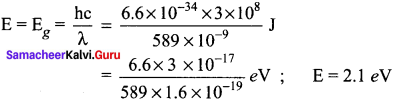
Question 2.
In PNP transistor circuit, the collector current is 10 mA. If 90% of the holes reach the collector, find emitter and base currents.
Solution:
Here, IE = 10 mA
As 90% of the holes reach the collector, so the collector current.
IC = 90% of IE
IC = \(\frac { 90 }{ 100 }\) IE
IE = \(\frac { 100 }{ 90 }\) IC = \(\frac { 100 }{ 90 }\) x 10
IE ≃ 11mA
Base current, IB = IE – IC = 11 – 10
IB = 1 mA.
![]()
Question 3.
In the circuit, the value of β is 100. Find IB, VCE, VBE and VBC, when IC = 1.5 mA. The transistor is in active, cut off or saturation state?
Solution:
β = 100; IC = 1.5 mA= 1.5 x 10⁻³ A, VCC = 24 V
β = \(\frac {{ I }_{ C }}{{ I }_{ B }}\)
IB = \(\frac {{ I }_{ C }}{β}\) = \(\frac { 1.5\times { 10 }^{ -3 } }{ 100 } \) = 15 μA
To calculate VCE, We apply Kirchhoff’s rule to loop CEFDC, therefore
VCC = IC x 4.7 kΩ + VCE
24 = 1.5 x 10-3 x 4.7 10-3 + VCE
VCE = 24 – 7.05 = 16.95 V
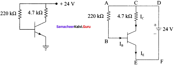
Again, applying Kirchhoff’s rule to loop ABEFDCA, We get,
VCC = IB x 220 kΩ + VBE
VCC = 15 x 10-6 x 220 x 10-3 + VBE
VBE = 24 -3.3
VBE = 20.7 V
Going along loop ABCA, we get
IB x 220 kΩ + VBC = Ic x 4.7 kΩ
15 x 10-6 x 220 x 103 + VBc = 1.5 x 10-3 x 4.7 x 103
VBC = 7.05 -3.3 = 3.75 V
As VCE < VBE, both the junctions are forward biased. So, the transistor is in the saturation state.
Question 4.
A transistor has α = 0.95. If the emitter current is 10 mA, what is (a) the collector current, (b) the base current and (c) gain β?
Solution:
Here, α = 0.95, IE = 10 mA
(a) α = \(\frac {{ I }_{ C }}{{ I }_{ E }}\) ⇒ IC = αIE = 0.95 x 10 = 9.5 mA
(b) IB = IE – IC = 10 – 9.5 = 0.5 mA
(c) β = \(\frac { α }{ 1-α }\) = \(\frac { 0.95 }{ 0.05 }\) = 19.
Question 5.
For a BJT, the common-base current gain α = 0.98 and the collector base junction reverse bias saturation current IC0= 0.6 μA. This BJT is connected in the common emitter mode and operated in the active region with a base drive current IB = 20 μA. Find the collector current IC for this mode of operation.
Solution:
α = 0.98 and IC0= 0.6 μA
Collector current,
β = \(\frac { α }{ 1-α }\) = \(\frac { 0.98 }{ 1-0.98 }\) = 49
Thus,
IC = (49 x 20) + (50 x 0.6) = 980 + 30 = 1010 μA
IC = 1.01 μA.
![]()
Question 6.
An NPN BJT having reverse saturation current IS = 10-15 A is biased in the forward active region with VBE = 700 mV and the current gain (β) may vary from 50 to 150 due to manufacturing variations. What is the maximum emitter current (in μA)
Solution:
IS = 10-15 A
VBE = 700
VT = 25 mV
β range from 50 to 150
IC = I0 e(VBE/VT)
IE = \(\frac { β+1 }{ β }\) IC
IE = \(\frac { β+1 }{ β }\) IS eVBE/VT
IE will be maximum when β is 50
= 1.02 × 10⁻¹⁵ × e700 × 10-3/25 × 10-3
IE = 1475 μA